(2017) Nanostructured Semiconductor Materials for, Dye-Sensitized Solar Cells+
VAL |
|
Offline

Мэтр, проФАН любви... proFAN of love
    
Профиль
Группа: Администраторы
Сообщений: 37438
Пользователь №: 1
Регистрация: 6.03.2004

|
(2017) Nanostructured Semiconductor Materials for Dye-Sensitized Solar CellsИсточники: - http://downloads.hindawi.com/journals/jnm/2017/5323164.pdf- https://www.hindawi.com/journals/jnm/2017/5323164/- Journal of Nanomaterials, Volume 2017, Article ID 5323164, 31 pages DOI: 10.1155/2017/5323164 Авторы: Carmen Cavallo, Francesco Di Pascasio, Alessandro Latini, Matteo Bonomo, and Danilo Dini QUOTE | Abstract
Since O’Regan and Grätzel’s first report in 1991, dye-sensitized solar cells (DSSCs) appeared immediately as a promising low-cost photovoltaic technology. In fact, though being far less efficient than conventional silicon-based photovoltaics (being the maximum, lab scale prototype reported efficiency around 13%), the simple design of the device and the absence of the strict and expensive manufacturing processes needed for conventional photovoltaics make them attractive in small-power applications especially in low-light conditions, where they outperform their silicon counterparts. Nanomaterials are at the very heart of DSSC, as the success of its design is due to the use of nanostructures at both the anode and the cathode. In this review, we present the state of the art for both N-type and P-type semiconductors used in the photoelectrodes of DSSCs, showing the evolution of the materials during the 25 years of history of this kind of devices. In the case of -type semiconductors, also some other energy conversion applications are touched upon. |
Присоединённое изображение
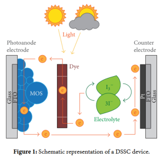
--------------------
|
|
|
VAL |
|
Offline

Мэтр, проФАН любви... proFAN of love
    
Профиль
Группа: Администраторы
Сообщений: 37438
Пользователь №: 1
Регистрация: 6.03.2004

|
QUOTE | 1.1. Introduction.
A dye-sensitized solar cell (DSSC) is asemiconductor-based photovoltaic device that directly con-verts both artificial and natural (solar) radiation into electriccurrent. In contrast to the conventional systems, where thesemiconductor assumes both the tasks of light absorption andcharge carrier separation and transport, the two functionsare separated in a DSSC. In a conventional DSSC, light isabsorbed by a sensitizer, which is anchored to the surfaceof a wide band gap𝑛-type semiconductor [1]. Often referredto as a Gr ̈atzel cell, this hybrid device was first reported tothe scientific world in 1991 by the seminal publication ofBrian O’Regan and Michael Gr ̈atzel presenting a device madeof sensitized nanocrystalline TiO2with a power conversionefficiency of 7.1% [2]. DSSCs constitute probably the cheapestphotovoltaic technology today available and their efficiencyhas been constantly improved in the last 25 years. Theconfirmed efficiency record is 11.9% [3], achieved by theSharp company. |
QUOTE | herefore, this section of the present paper aims atbringing together the various contributions brought about byresearchers to improve the efficiency of the𝑛-type sensitized semiconductors for DSSCs. Moreover, the detailed discussion of the role of band gap,morphology,composition, and doping of𝑛-type semiconductors for the development ofefficient photoanodes will be reported. Several contributions are summarized here with the description of nanostructures (0D, 1D, 2D, 3D, and mesoporous nanostructures) and of the effect of doping of photoanodes materials (mostly TiO2andZnO) on the performances of DSSCs. |
--------------------
|
|
|
VAL |
|
Offline

Мэтр, проФАН любви... proFAN of love
    
Профиль
Группа: Администраторы
Сообщений: 37438
Пользователь №: 1
Регистрация: 6.03.2004

|
QUOTE | 1.3. Photoanode Materials for 𝑛-Type DSSC.
The conduction band edge𝐸CBofthephotoanodematerialshould match with that of the excited dye molecules. To effi-ciently collect the photogenerated electrons, the photoanodeshould have high charge carrier mobility.Desirable properties of the material are also the ease topreparation, stability, low-cost, and environmental friendli-ness. These properties are the defining characteristics of anideal photoanode
|
QUOTE | Полупроводниковые наноструктурированные пленки являются основным ядром фотоанодов DSSCs. Основными проблемами в DSSCs являются процессы рекомбинации заряда и их относительно низкая светопоглощающая способность. Фотоанод выполняет двойную функцию как опоры для сенсибилизатора, так и носителя фотогенерированных электронов от сенсибилизатора к внешней цепи [17]. Фотоанодный материал не должен поглощать видимый свет и должен иметь достаточно высокую площадь поверхности для оптимального поглощения (adsorption). В полупроводниковая терминология, верхняя часть валентной полосы и нижняя часть зоны проводимости называются кромкой полосы валентности и кромкой полосы проводимости соответственно. Энергия края зоны проводимости обозначается как 𝐸CB; аналогично, энергия края валентной зоны обозначается как 𝐸VB. Разность энергий между этими уровнями называется межзонной щелью (𝐸𝑔). Размер этой запрещенной зоны является, пожалуй, самым важным свойством полупроводника, так как он влияет на все важнейшие электронные свойства материала [18]. Край зоны проводимости 𝐸Cb of the photoanode material должен совпадать с краем возбужденных молекул красителя. Для эффективного сбора фотогенерированных электронов фотоанод должен обладать высокой подвижностью носителей заряда. Желательными свойствами материала являются также легкость приготовления, стабильность, низкая стоимость и экологичность. Эти свойства являются определяющими характеристиками идеального фотоанода. |
--------------------
|
|
|
0 Пользователей читают эту тему (0 Гостей и 0 Скрытых Пользователей)
0 Пользователей: